First, let's discuss the causes of low-frequency vibrations.
Repeated tests have shown that low-frequency vibrations are primarily caused by the resonances of the building. The construction specifications for industrial and civil buildings are generally similar in terms of floor height, depth, span, beam and column sections, walls, floor beams, raft slabs, etc. Although there may be some differences, particularly regarding low-frequency resonances, common characteristics can be identified.
Here are some patterns observed in building vibrations:
1. Buildings with linear or point-shaped floor plans tend to exhibit larger low-frequency resonances, while those with other shapes such as T, H, L, S, or U have smaller resonances.
2. In buildings with linear floor plans, vibrations along the long axis are often more pronounced than those along the short axis.
3. In the same building, the first floor without a basement typically experiences the smallest vibrations. As the floor height increases, the vibrations worsen. The vibrations in the first floor of a building with a basement are similar to those in the second floor, and the lowest vibrations are typically observed in the lowest level of the basement.
4. Vertical vibrations are generally larger than horizontal vibrations and are independent of the floor level.
5. Thicker floor slabs result in smaller differences between vertical and horizontal vibrations. In the majority of cases, vertical vibrations are larger than horizontal vibrations.
6. Unless there is a significant vibration source, vibrations within the same floor of a building are generally consistent. This applies to locations in the middle of a room as well as those near walls, columns, or overhead beams. However, even if measurements are taken at the same location without any movement and with a few minutes interval, the values are likely to differ.
Now that we know the sources and characteristics of low-frequency vibrations, we can take targeted improvement measures and make advanced assessments of the vibration conditions in certain environments.
Improving low-frequency vibrations can be costly, and sometimes it is not feasible due to environmental constraints. Thus, in practical applications, it is often advantageous to choose or relocate to a better site for operating an electron microscope laboratory.
Next, let's discuss the impact of low-frequency vibrations and potential solutions.
Vibrations below 20 Hz have a significant disruptive effect on electron microscopes, as depicted in the following figures.
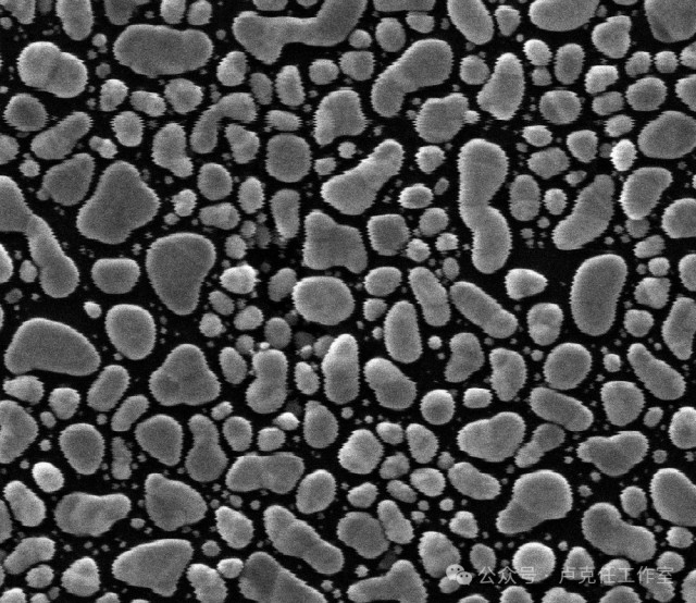
Image 1
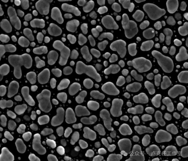
Image 2
Image 1 and Image 2 were taken by the same Scanning Electron Microscope (both at 300kx magnification). However, due to the presence of vibration interference, Image 1 has noticeable jaggedness in the horizontal direction (in segments), and the clarity and resolution of the image are significantly reduced. Image 2 is the result obtained from the same sample after eliminating the vibration interference.
If the test results indicate that the location where the microscope is to be installed has excessive vibrations, appropriate measures must be taken; otherwise, the microscope manufacturer cannot guarantee that the performance of the microscope after installation can meet the optimal design standards. Generally, several methods can be chosen to improve or solve the issue, such as using an Anti-Vibration Foundation, Passive-Vibration Isolation Platform, or Active-Vibration Isolation Platform.
An Anti-Vibration Foundation requires on-site construction and special measures need to be taken (such as having an elastic cushion layer at the bottom and surrounding areas). Conventional construction methods may potentially increase low-frequency vibrations (below 20Hz). The construction process involving a large amount of construction materials coming in and out may inevitably affect the surrounding environment. A schematic diagram of an Anti-Vibration Foundation can be seen in Image3.
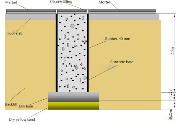
Image3
A concrete vibration isolation platform with a mass of around 50 tons generally achieves a vibration reduction effect of -2 to -10dB at frequencies above 2Hz. The larger the mass of the concrete vibration isolation platform, the better the vibration reduction. If conditions permit, it should be made as large as possible.
Based on multiple tests conducted in different locations, vibration isolation platforms weighing less than 5 tons exhibit resonance in the low-frequency range of 1-10Hz, which increases vibration. Those weighing less than 20 tons are ineffective, and the effective range starts at over 30 tons. No data is available for 30-40 tons, so it is advisable to avoid weights below 50 tons. A university in Beijing has achieved good results with a vibration isolation platform weighing around 100-200 tons. In a research institute in Chongqing, the ground concrete was directly poured on massive rocks, resulting in minimal vibration.
Among passive vibration dampers, commonly used options like rubber, steel springs, and air springs (cylinders) provide poor performance in the low-frequency range below 20Hz. They often amplify vibrations due to resonance, so they are not considered suitable.
Only magnetic dampers show acceptable low-frequency performance, but their performance is still far inferior to active dampers (similar to the vibration reduction effect of concrete vibration isolation platforms). Figure 4 compares the effectiveness of several methods.
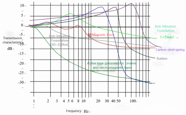
Figure 4
Upon careful observation of Figure 4, we can draw the following conclusions:
1. The resonance frequency (fh) of the carbon steel spring is approximately 50 Hz. It does not provide any damping effect below 70 Hz and, in fact, amplifies the vibration due to resonance. The rubber pad has an fh of approximately 25 Hz and does not provide any damping effect below 35 Hz, also amplifying the vibration due to resonance.
2. Concrete dampers with a capacity below 5 tons exhibit resonance below 10 Hz and are often less effective than not using a damper at all.
3. Air springs have an fh of approximately 15 Hz, providing good damping above 25 Hz and excellent damping above 40 Hz. They are widely used for vibration isolation in precision equipment such as optical platforms. However, they exhibit significant resonance below 20 Hz, making them unsuitable for damping electron microscopes (although some electron microscopes do use air springs as a last resort).
4. Magnetic dampers provide satisfactory low-frequency damping and can be used when strict requirements are not imposed.
5. Various active dampers achieve excellent damping effects. Their resonance frequencies can be below 1 Hz, and they can provide damping up to -10 to -22 dB in the 2-10 Hz range, making them ideal for applications requiring effective damping in the low-frequency range.
In general, vibrations below 20 Hz are considered to have a significant impact on electron microscopes and are difficult to mitigate. Since most people cannot perceive vibrations below 20 Hz, it often leads to a misconception that there is no vibration when significant low-frequency vibrations are present.
Passive dampers utilize the physical properties of damping devices, such as their mass and inherent vibration transmission characteristics, to isolate and attenuate external vibrations affecting the electron microscope. The working principle of passive dampers can be referenced in Figure 5.
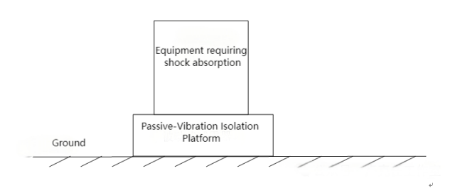
Figure 5
The working principle of active dampers is significantly different from passive dampers. Various types of active dampers have similar working principles, which involve a three-dimensional sensor detecting external vibrations in three directions. The sensor sends the information to a PID (Proportional-Integral-Derivative) controller, which generates control signals with equal amplitude but opposite phase. These control signals are then used by an actuator to generate internal vibrations with equal amplitude and opposite phases to counteract or reduce the external vibrations. The working principle of active dampers can be referred to as shown in Figure 6.
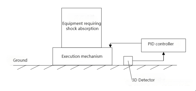
Figure 6
Active dampers commonly used include piezoelectric ceramic dampers, pneumatic dampers, and electromagnetic dampers. Their differences mainly lie in the actuation mechanism, while 3D detectors and PID controllers are relatively similar.
Piezoelectric Ceramic Dampers:
They utilize the piezoelectric effect of the ceramic material to generate three-dimensional internal vibrations with equal amplitude and opposite phase.
Pneumatic Dampers:
Controlled by a PID controller, the inlet and outlet valves modulate the continuous compressed air in a special cylinder to generate three-dimensional internal vibrations with equal amplitude and opposite phase.
Electromagnetic Dampers:
The PID controller controls three sets of electromagnetic coils to generate three-dimensional internal vibrations with equal amplitude and opposite phase.
Active dampers can achieve vibration reduction effects of approximately -22 to -28 dB above 20 Hz (although there have been claims of achieving -38 dB, they are mostly unsubstantiated).
Different types of active dampers also have significant price differences. Generally, the dampers are prepared before the electron microscope is installed and are installed simultaneously with the microscope.
In addition, under specific conditions, a vibration isolation trench can also achieve good damping effects.
Figure 7 depicts a situation where the vibration isolation trench is.
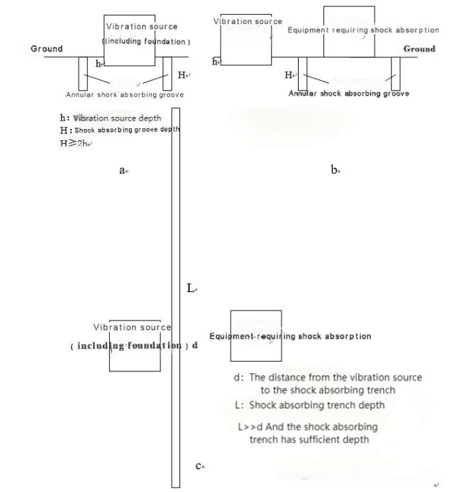
Figure 7
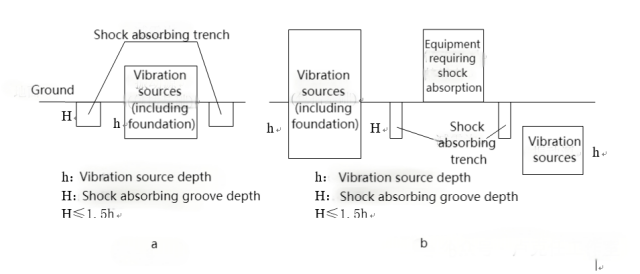
Figure 8
Figure 8 represents an ineffective scenario for a vibration trench.
In general, the deeper the vibration trench, the better the damping effect (the width of the trench has little impact on the damping effect). Here is a comparison of several common damping methods:
|
Type
|
Carbon Steel
Spring
|
Rubber
Dampers
|
Anti-Vibration
Foundation
|
Magnetic
Dampers
|
Air Spring
(Cylinder)
|
Active
Dampers
|
|
Price
|
Lowest
|
Low
|
Medium
|
Low
|
High
|
Highest
|
|
Damping
Performance
|
1~5Hz
|
Poor
|
Poor
|
Medium
|
Poor
|
Poor
|
Excellent
|
|
5~20Hz
|
Poor
|
Poor
|
Medium
|
Medium
|
Poor
|
Excellent
|
|
20~50Hz
|
Poor
|
Medium
|
Medium
|
Good
|
Medium
|
Excellent
|
|
>50Hz
|
Good
|
Good
|
Medium
|
Good
|
Good
|
Good
|
|
Installation and
Adjustment Difficulty
|
Easy
|
Easy
|
Difficult
|
Easy
|
Medium
|
Difficult
|
|
Energy Consumption
|
None
|
None
|
None
|
None
|
A small amount of compressed
gas
|
>300w
|
|
Routine Maintenance
|
None
|
None
|
None
|
None
|
Required
|
Required
|
|
Appearance
|
Integrated/
Separate
|
Integrated/
Separate
|
Concealed
underground
|
Separate
|
Separate +
Flat panel
|
Integrated/
Separate+
Flat panel
|